4 GHz PROGRAMMABLE ATTENUATOR
MODEL PA1
Features
- DC to 4 GHz bandwidth
- 1O Bit (1024 step) range
- Low profile
- 0625 dB step
- Constant phase
- Precise repeatability
- 50 ohm matched I/O
- High-speed TTL control
PRODUCT DESCRIPTION .... SPECIFICATIONS .... PROGRAMMING .... TRANSFER CHARACTERISTICS .... PRICING AND AVAILABILITY ... HOME PAGE
The PA1 is a single channel programmable attenuator designed for adjusting the amplitude of radio and microwave signals of bandwidths from DC to 4 GHz.
This device has low impedance mismatch, high bandwidth, wide dynamic range and is capable of rapid state change. The PA1 can be an attractive alternative to either the manually operated microwave attenuator switches, which are expensive and are switched very slowly, or the relay attenuators which are expensive and wear out quickly.
Attenuation is controlled in standard steps of 0.0625 dB. The 10 bit programmable range results in the full 210=1024 steps yielding a dynamic range of O to 63.9375dB. Non-standard custom step sizes are available.
The PA1 is specifically designed to minimize any phase shift between attenuator states. The maximum phase deviation between any attenuation states is determined by the maximum delay shift of +/- 10 ps.. The phase shift between consecutive attenuation states is typically 2 to 3 picoseconds. This device is specially calibrated to maintain high accuracy at the control word major-carries so that attenuation states do not overlap or have large errors at these points.
The PA1 employs all GaAs passive microwave switched-line and switched-element techniques. Lines are switched in a series configuration so that each attenuation value occurs additively with any other switched-in attenuation. While GaAs FETS are used as the switching devices, both thick and thin film resistor components are used as attenuation elements. This provides a much higher degree of thermal stability as compared to programmable attenuators which use attenuation elements made of silicon or GaAs. The cumulative temperature coefficient is less than +/-0.01 dB/'F. This also lends to an outstandingly low repeatability error of less than +/-0.02 dB.
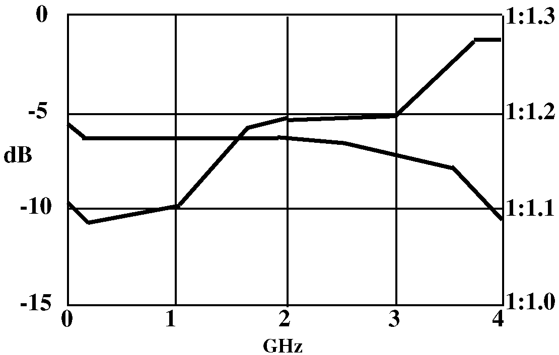
The PA1 is calibrated to maintain a high degree of accuracy over the widest range of frequencies. Below 2.5 GHz, this results in accuracy better than 0.2+/-1% dB.. The signal is DC coupled therefore has no lower band limit. Since no active elements are used, saturation effects are reduced so that input power of as high as 20 dBm may be used without appreciable compression. The attenuator's I/O provide a good match of 50 ohms, relative to ground, yielding a VSWR of less than 1.25 from DC to 2.5 GHz and less than 1.35 to 4 GHz. This helps maintain accuracy in applications where the signal source and termination are not well matched over the band.
RF inputs and output are connected by SMA jacks while data and control signals are connected by a standard 25 pin D-type connector plug. Power is connected through the D-sub connector. This device is provided in a low profile rugged aluminum housing and requires a single, low power, 5V supply making this instrument very easy to use.
Fast, ACT control logic is used to support applications requiring rapid attenuation state change. This allows programming rates in excess of 50 MHz. If higher programming speeds are required, or if 110 ohm input terminations to TTL threshold are desired, contact the manufacturer.
TRANSFER CHARACTERISTICS
The diagram above shows the typical transfer characteristics for attenuation state set to 0 dB. Also shown is the typical maximum. VSWRs between various attenuation states.
The attenuation is equal to the 0.0625 dB step size times the 10 bit control word number. Each of the 10 bits corresponds to a separate attenuator element. These 10 elements are connected in a series configuration to give 1024 combinations 0 to 63.9375dB. The latch enable line (LE) is active (low) to latch the control word. The control word need not be latched if the user wishes to operate the latch transparently. Simply keep the latch line high and the attenuation state will follow the applied data.
PIN DIAGRAM
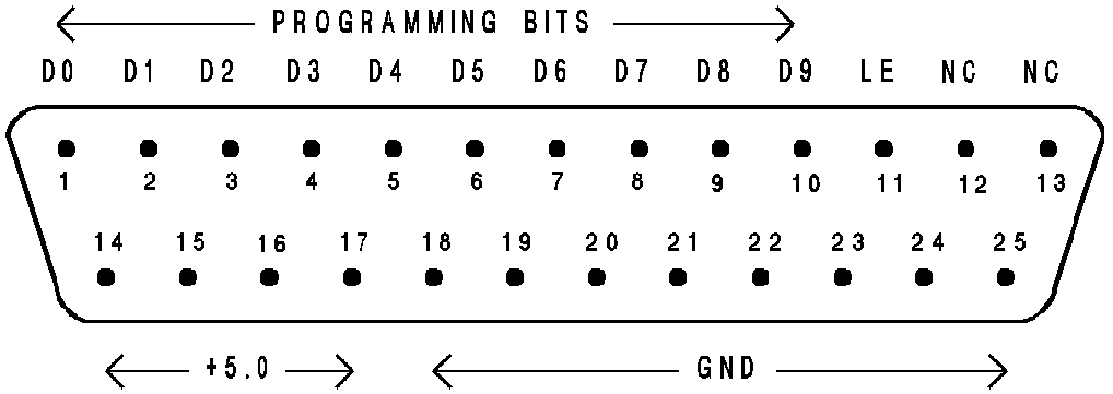
25 pin D-type subminiature connector
POWER REQUIREMENTS
The PA1 uses a single 5V supply. The current requirement is 200 mA but it is typically below 100 mA at low programming rates. Internal supply voltages are regulated to eliminate supply noise coupling to the signal path. The input buffer uses the 5V supply directly all other internal voltages are generated from the 5V supply in order to simplify power-up.
ABSOLUTE MAXIMUM RATINGS
(beyond which damage may occur)
![]() GigaBaudics
5266 Hollister Ave. Ste 221 ●
Goleta, CA 93111 ● (805) 687-5934
GigaBaudics
5266 Hollister Ave. Ste 221 ●
Goleta, CA 93111 ● (805) 687-5934
Please use E-Mail for any correspondences, either technical or administrative, at address postman@gigabaudics.com